Mastering Energy Band Diagrams: A Deep Dive Into Solid-State Physics
Welcome to your one-stop guide on energy band diagrams! Whether you’re a physics student, an engineering enthusiast, or just curious about how materials conduct electricity, this article will walk you through the fundamentals, key concepts, and practical applications of energy band diagrams in an engaging and approachable way. By the end, you’ll confidently interpret diagrams, understand their importance in modern technology, and know how to leverage this knowledge in your projects or studies.
What is an Energy Band Diagram?
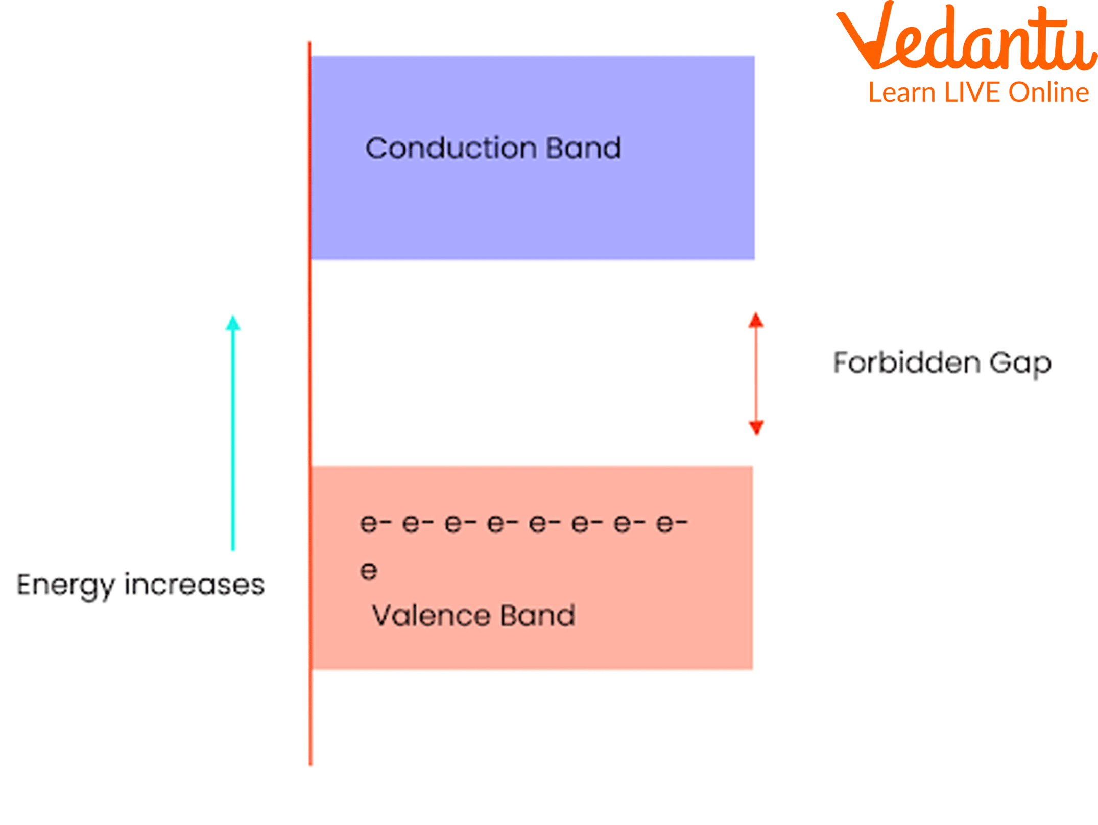
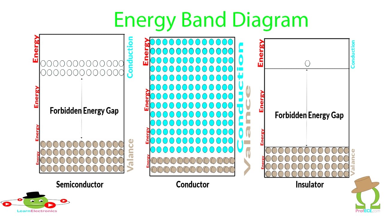
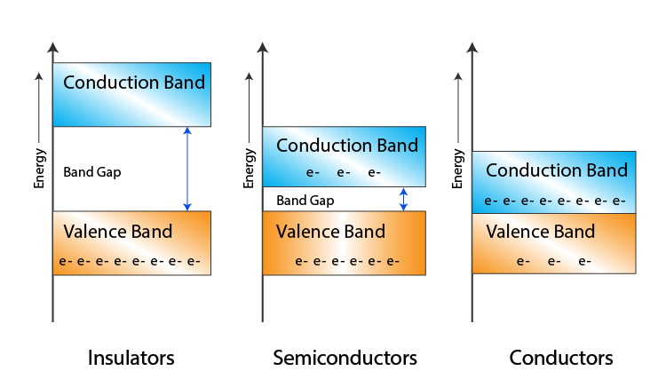
An energy band diagram is a visual representation of the allowed energy levels of electrons within a crystalline solid. In these diagrams, the horizontal axis typically shows the position or momentum of electrons, while the vertical axis indicates energy. The diagram delineates the valence band (filled with electrons) and the conduction band (available for free electron movement), separated by the band gap. Understanding this relationship is crucial because it determines whether a material behaves as a metal, semiconductor, or insulator. The diagram also illustrates how electrons transition between bands when energy is applied, a process foundational to devices like diodes, transistors, and solar cells.
Key Features of Silicon’s Band Diagram
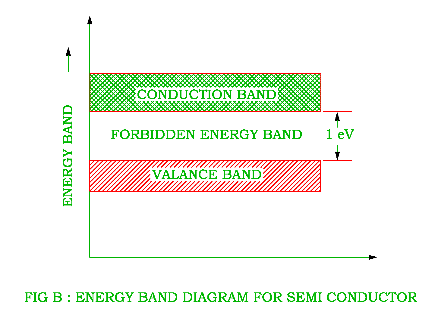
Silicon, the workhorse of the electronics industry, showcases a classic semiconductor band structure. The valence band is completely filled at absolute zero, while the conduction band remains empty. The energy gap, or band gap, between them is about 1.1 eV—just the right size for manipulating electron flow at room temperature. Below is a detailed view of silicon’s energy band diagram:

The diagram reveals several critical details:
- Valence Band Maximum (VBM): The highest energy level occupied by electrons at zero Kelvin.
- Conduction Band Minimum (CBM): The lowest available energy state for electrons to move freely.
- Band Gap (Eg): The energy difference that electrons must acquire to jump from VBM to CBM.
- Intrinsic Carrier Concentration: At equilibrium, a small fraction of electrons occupy the conduction band, while holes populate the valence band, enabling conductivity.
By adjusting external conditions—such as temperature or doping—you can shift these bands, effectively tuning silicon’s electrical properties. This ability to engineer band structure is why silicon remains at the heart of virtually every semiconductor device.
How to Read Any Energy Band Diagram
Reading a band diagram is akin to decoding a map. Here’s a quick checklist:
- Identify the Bands: Look for shaded or colored regions representing the valence and conduction bands. The space between them is the band gap.
- Determine the Band Gap: Measure the vertical distance between the VBM and CBM. A smaller gap typically means the material behaves more like a conductor.
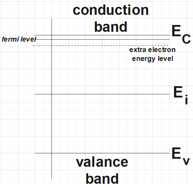
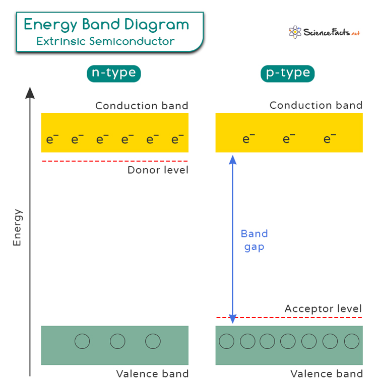
- Check for Doping Levels: Extra lines or markers indicate donor or acceptor levels introduced by doping. These levels appear within the band gap and shift the Fermi level.
- Observe the Fermi Level: The Fermi level indicates the probability of electron occupancy at a given energy. In intrinsic materials, it lies near the middle of the band gap; in doped materials, it shifts toward the conduction or valence band.
- Look for Excited States: Transitions, often represented by arrows, show how electrons absorb or emit photons, crucial for devices like LEDs and photodetectors.
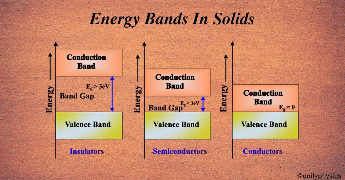
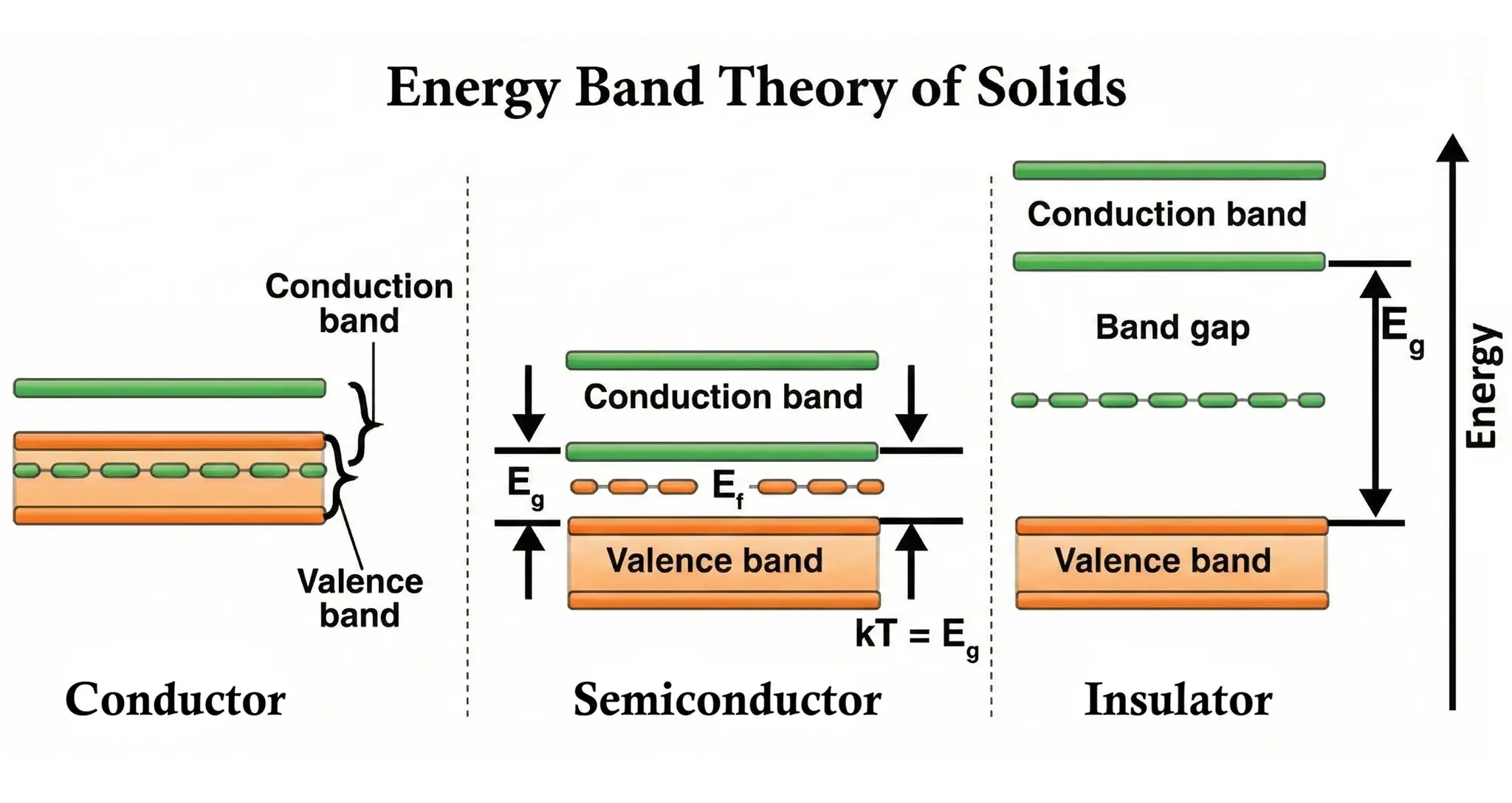
Let’s examine a generic depiction of energy levels in solids that highlights these elements:

This image provides a clear snapshot of the key components, making it easier to apply the checklist to more complex diagrams you may encounter in research or coursework.
Applications in Modern Technology
Energy band diagrams are not just academic tools; they directly inform the design and operation of countless technologies:
- Semiconductor Devices: Transistors, MOSFETs, and diodes rely on precise band engineering to control charge carrier flow.
- Optoelectronics: LEDs and laser diodes depend on band-to-band recombination to emit light. By tuning band gaps, manufacturers produce devices across the visible spectrum.
- Photovoltaics: Solar cells harness photons to excite electrons across the band gap. Understanding band alignment between layers optimizes charge separation and collection.
- Material Discovery: New 2D materials and topological insulators are evaluated by inspecting their band structures for exotic properties like Dirac cones or edge states.
Each application demonstrates how band diagram insights translate into functional performance. Engineers routinely simulate band structures using software like VASP or Quantum ESPRESSO to predict material behavior before experimental fabrication.
Tips for Mastering Band Diagrams
Here are some practical strategies to deepen your understanding:
- Practice with Real Data: Download band diagrams from research papers and annotate key features. The more you dissect, the more intuitive the patterns become.
- Relate to Electronic Band Theory: Review the quantum mechanical basis—Bloch’s theorem, Brillouin zones, and band folding—to contextualize the visual data.
- Use Interactive Simulations: Platforms like PhET and the MIT OpenCourseWare provide interactive band diagram tools that let you tweak parameters and instantly see the effects.
- Connect to Device Physics: Map how band bending at p-n junctions or heterostructures influences carrier transport, reinforcing the link between diagram and device operation.
- Stay Updated on Emerging Materials: Keep an eye on recent publications, especially in 2D semiconductors, to see how novel band structures challenge traditional concepts.
Conclusion
Energy band diagrams are the language of solid-state physics, bridging the microscopic quantum world with macroscopic electronic devices. By mastering how to read and interpret these diagrams, you unlock the ability to predict material behavior, innovate in device design, and stay at the forefront of technology. Whether you’re analyzing silicon’s classic band gap or exploring cutting-edge materials, the insights gained from energy band diagrams are invaluable. Dive into the diagrams, experiment with simulations, and let the band structure guide your journey into the exciting realm of modern electronics and beyond.
Energy Band Diagram Of Semiconductor | PPTX

Energy band diagram of semiconductor | PPTX
Energy Band Diagram Toshiba | Semiconductor Band Diagram – GQUGX

Energy Band Diagram Toshiba | Semiconductor Band Diagram – GQUGX
How To Draw Band Diagrams - Crazyscreen21

How To Draw Band Diagrams - Crazyscreen21
Energy Bands Explained: Basics, Types & Importance
Energy Bands Explained: Basics, Types & Importance
Energy Band Diagram

Energy Band Diagram
Energy Band Diagaram ( Conductor, Semiconductor And Insulator
Energy Band Diagaram ( Conductor, Semiconductor and Insulator ...
Band Theory Of Solids: Learn Energy Bands In Solids, Importance

Band Theory of Solids: Learn Energy Bands in Solids, Importance
Energy Bands: Classification & Explanation

Energy Bands: Classification & Explanation
Draw Energy Band Diagrams Of An N-type And P-type Semiconductor At
Draw energy band diagrams of an n-type and p-type semiconductor at ...
What Are Energy Bands In Solids At Barbara Fowler Blog
What Are Energy Bands In Solids at Barbara Fowler blog
Band Diagram Example At Justin Northcote Blog
Band Diagram Example at Justin Northcote blog
Energy Band Theory In Solids

Energy band theory in solids
Extrinsic Semiconductors: Definition, Types, And Band Diagram
Extrinsic Semiconductors: Definition, Types, and Band Diagram
Electrical Revolution: Energy Band Diagaram ( Conductor, Semiconductor

Electrical Revolution: Energy Band Diagaram ( Conductor, Semiconductor ...
Energy Bands Diagram | Band Diagram – TMCTHY

Energy Bands Diagram | Band diagram – TMCTHY
Energy Bands - Definition And Classification Of Energy Bands | Band Theory
Energy Bands - Definition and Classification of Energy Bands | Band Theory
Energy Bands Of Silicon

Energy Bands of Silicon
Circuit Diagram Of Intrinsic Semiconductor

Circuit Diagram Of Intrinsic Semiconductor
Conductor Energy Diagram
Conductor Energy Diagram
Definition And Classification Of Energy Bands - GeeksforGeeks

Definition and Classification of Energy Bands - GeeksforGeeks
Definition Of Energy Band Diagram - FEDINIT

Definition Of Energy Band Diagram - FEDINIT
Semiconductor, Energy Band Diagram

Semiconductor, Energy band diagram
Schematic Representation Of Energy Bands Within A Solid. | Download
Schematic representation of energy bands within a solid. | Download ...